
Designing your PCB
Welcome to the first part of your robot! This guide takes you from a blank KiCad project to a routed and checked Waypoint robot-controller PCB.
For this guide we’re using KiCad, an open source PCB design tool.
Start The Schematic
Section titled “Start The Schematic”First, open KiCad and create a project for your robot.
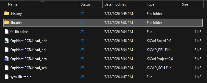
To start, import the needed symbols and footprints: How to Import KiCad Libraries. Symbols are the parts you place in the schematic. Footprints are the physical shapes that appear on the PCB.
After importing, your project should contain both library files:
Now open the schematic editor.
The schematic shows which pins connect to each other.
Press A to add a symbol. Search for WaypointCarePackage:DROK_BUCK_MODULE. If it appears, the symbol library is working.
The power section gives the board the voltages the robot needs and adds a power switch.
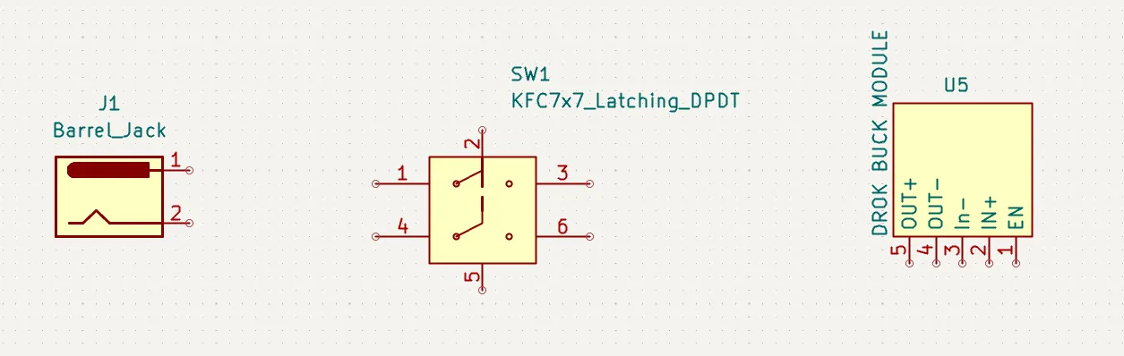
Press A and add:
Connector:Barrel_JackWaypointCarePackage:KFC7x7_Latching_DPDTWaypointCarePackage:DROK_BUCK_MODULE
Place them roughly like this:
Press P to add power symbols. Place +BATT, +9V, +5V, and GND.
Press W to draw wires. Wire the barrel jack, switch, buck converter, and power symbols to match the completed section below. The buck input and EN pin go to switched +9V, the buck negative pins go to GND, and the output goes to +5V.
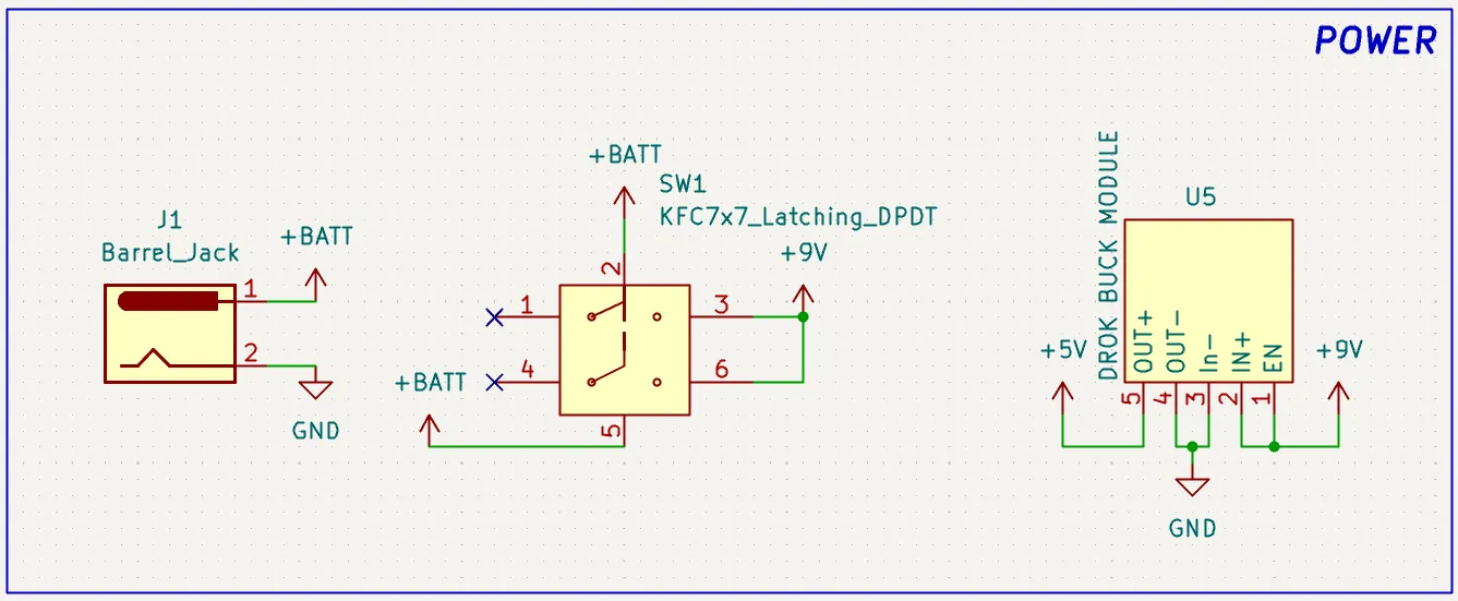
When you reach an unused pin, press Q to place a no-connect marker. That tells KiCad, and anyone reviewing your design, that the pin is intentionally unused.
Motor Drivers
Section titled “Motor Drivers”The motor drivers let the Raspberry Pi control the motors.
Press A and add two WaypointCarePackage:DRV8833_MODULE symbols and four Connector:Screw_Terminal_01x02 symbols.
Connect each DRV8833 to +9V and GND. Connect the four motor-output pairs to the four screw terminals, just like this:
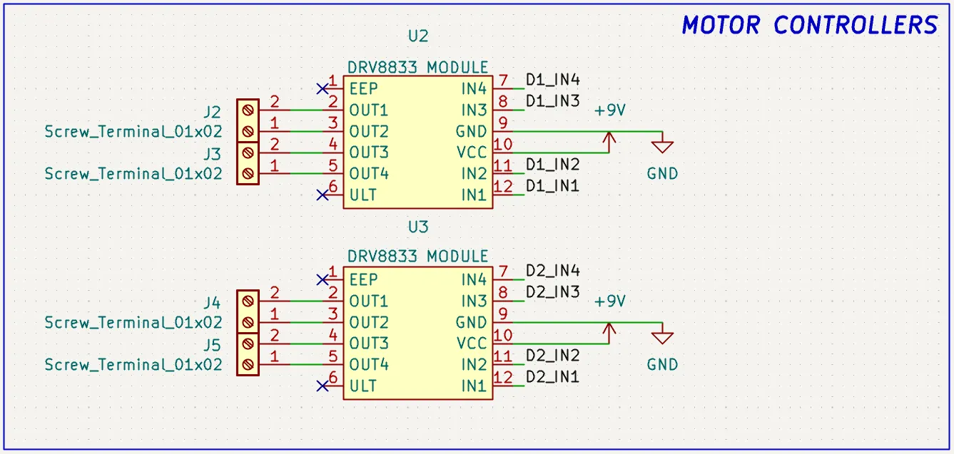
This is where labels are easier than long wires. Press L to add net labels for the motor inputs:
D1_IN1D1_IN2D1_IN3D1_IN4D2_IN1D2_IN2D2_IN3D2_IN4The MPU6050 lets the robot sense movement.
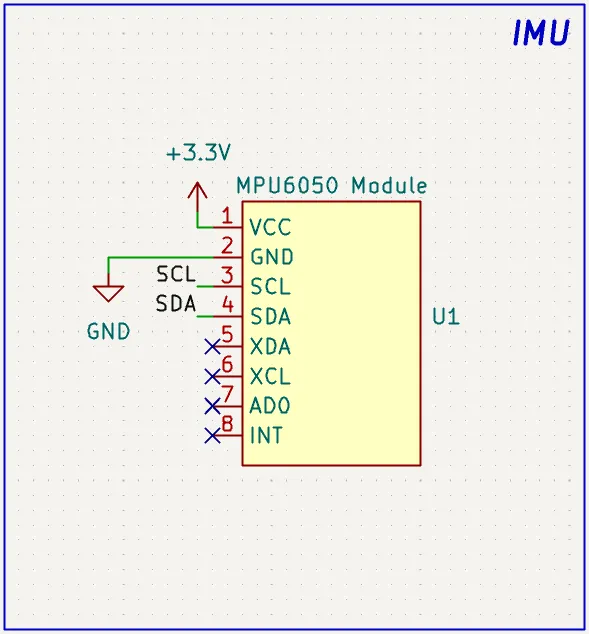
Press A and add WaypointCarePackage:MPU6050_MODULE. Connect VCC to +3.3V, connect GND, and label the I2C pins SDA and SCL. Mark unused pins with Q.
Raspberry Pi
Section titled “Raspberry Pi”The Raspberry Pi controls the motor drivers and communicates with the IMU.
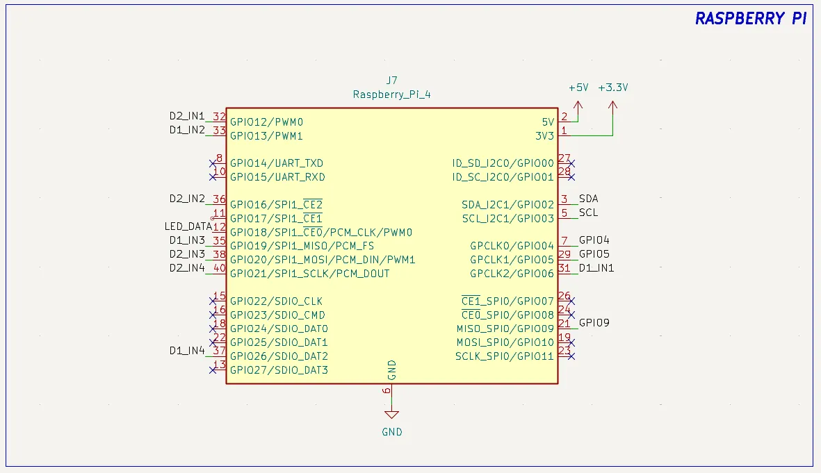
Press A and add Connector:Raspberry_Pi_4. This symbol gives you the standard 40-pin Raspberry Pi header.
Use this pinout while you connect the labels:
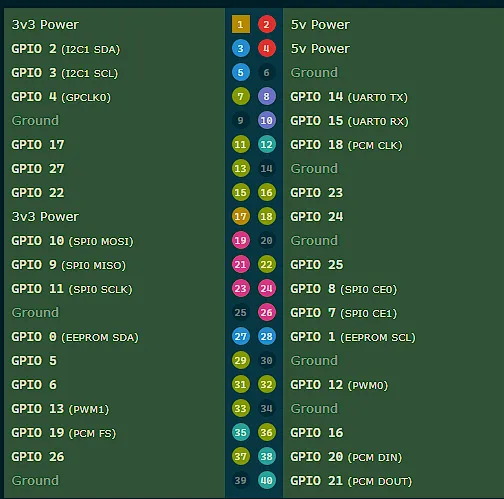
Connect +5V, GND, and the Pi 3.3V pin. Connect SDA to physical pin 3, SCL to physical pin 5, and the D1_IN* and D2_IN* labels to GPIO pins.
Bonus Feature And Mounting
Section titled “Bonus Feature And Mounting”Add a spare header or another small feature that makes the board yours.
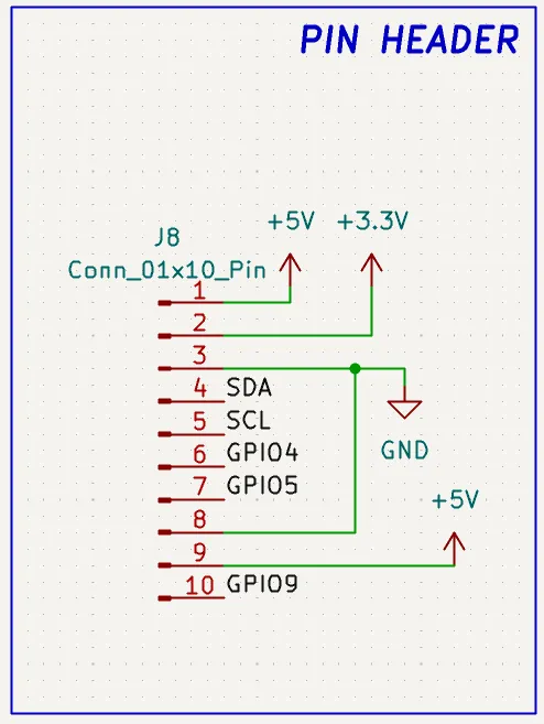
Press A and add a spare header such as Connector:Conn_01x10_Pin. For a smaller feature, use the matching pin count, like Connector:Conn_01x03_Pin for a 3-pin servo header. Wire useful pins such as GND, +5V, +3.3V, SDA, SCL, and extra GPIO.
Here’s an example breakout on Orphbot:
For a servo header, use this order:
GND+5VPWM-capable GPIOMost Raspberry Pi GPIO pins can do software PWM. GPIO12, GPIO13, GPIO18, and GPIO19 are easy PWM-capable choices.
Add M3 mounting holes with Mechanical:MountingHole.

Check And Assign Footprints
Section titled “Check And Assign Footprints”Run Inspect > Electrical Rules Checker. Fix real errors before moving into the PCB editor.
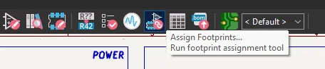
Footprints are the physical shapes that will appear on the PCB. Open the footprint assignment tool.
Some rows may be blank at first.
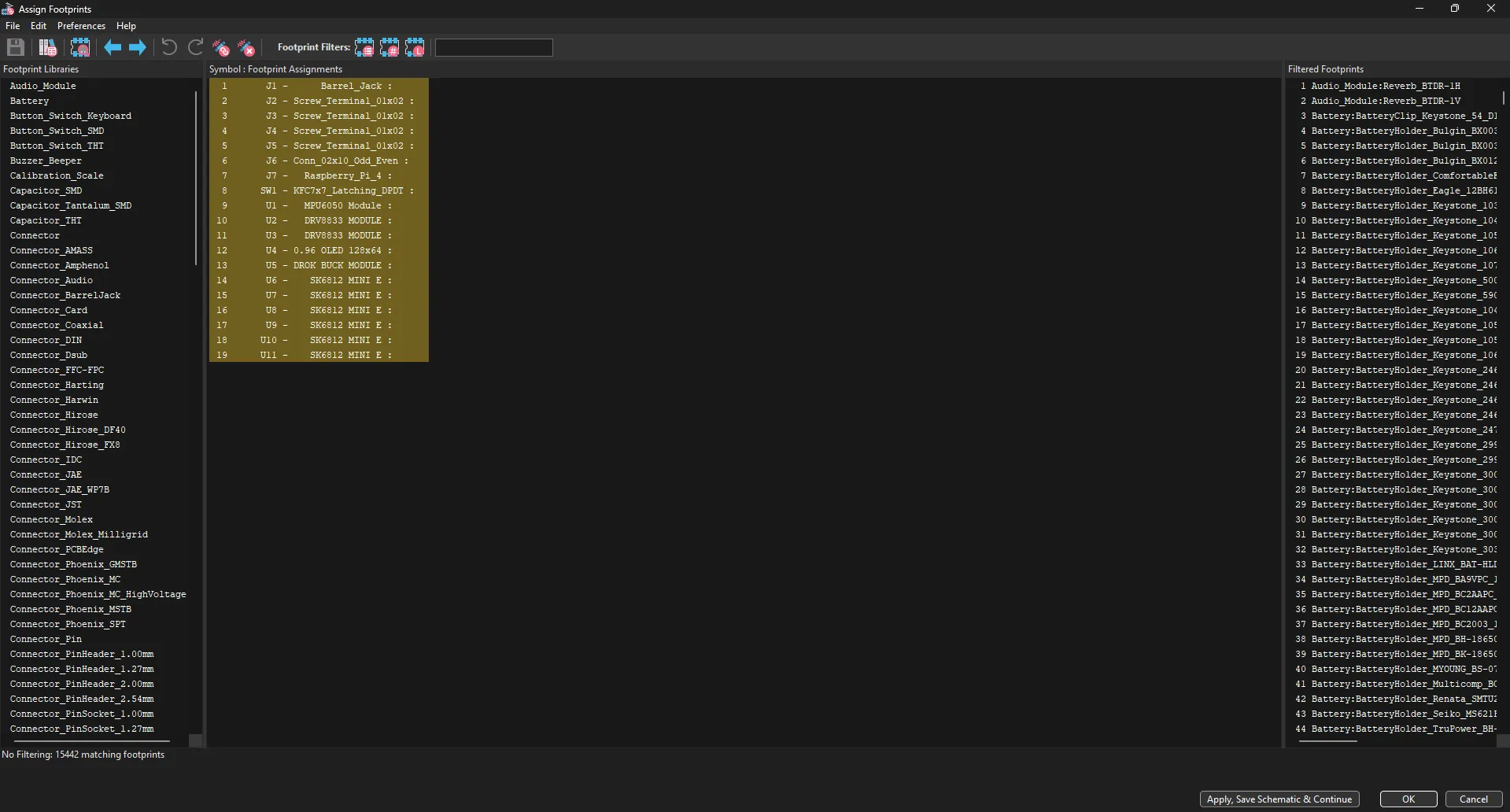
Use these assignments for the main parts you can find in your kit:
| Symbol | Footprint |
|---|---|
Connector:Barrel_Jack |
Connector_BarrelJack:BarrelJack_Horizontal |
WaypointCarePackage:KFC7x7_Latching_DPDT |
WaypointCarePackage:KFC7x7_Latching_DPDT_Blue |
WaypointCarePackage:DROK_BUCK_MODULE |
WaypointCarePackage:LOW_DROK_BUCK_MODULE |
WaypointCarePackage:DRV8833_MODULE |
WaypointCarePackage:DRV8833_MODULE |
Connector:Screw_Terminal_01x02 |
WaypointCarePackage:TerminalBlock_KF301-2P_P5.08mm_Blue |
WaypointCarePackage:MPU6050_MODULE |
WaypointCarePackage:LOW_MPU6050_MODULE |
Connector:Raspberry_Pi_4 |
WaypointCarePackage:MODULE_RASPBERRY_PI_ZERO_2_W |
Connector:Conn_01x#_Pin |
Connector_PinHeader_2.54mm:PinHeader_1x#_P2.54mm_Vertical |
Mechanical:MountingHole |
MountingHole:MountingHole_3.2mm_M3_Pad_Via |
These are the ones I picked:
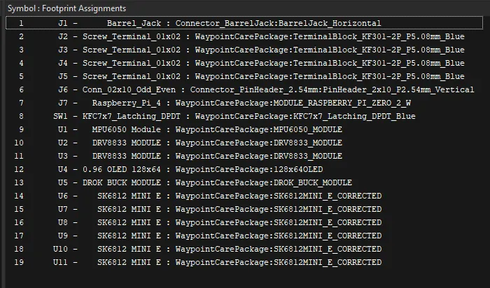
Apply the changes and save.
Place And Outline The PCB
Section titled “Place And Outline The PCB”Open the PCB editor.
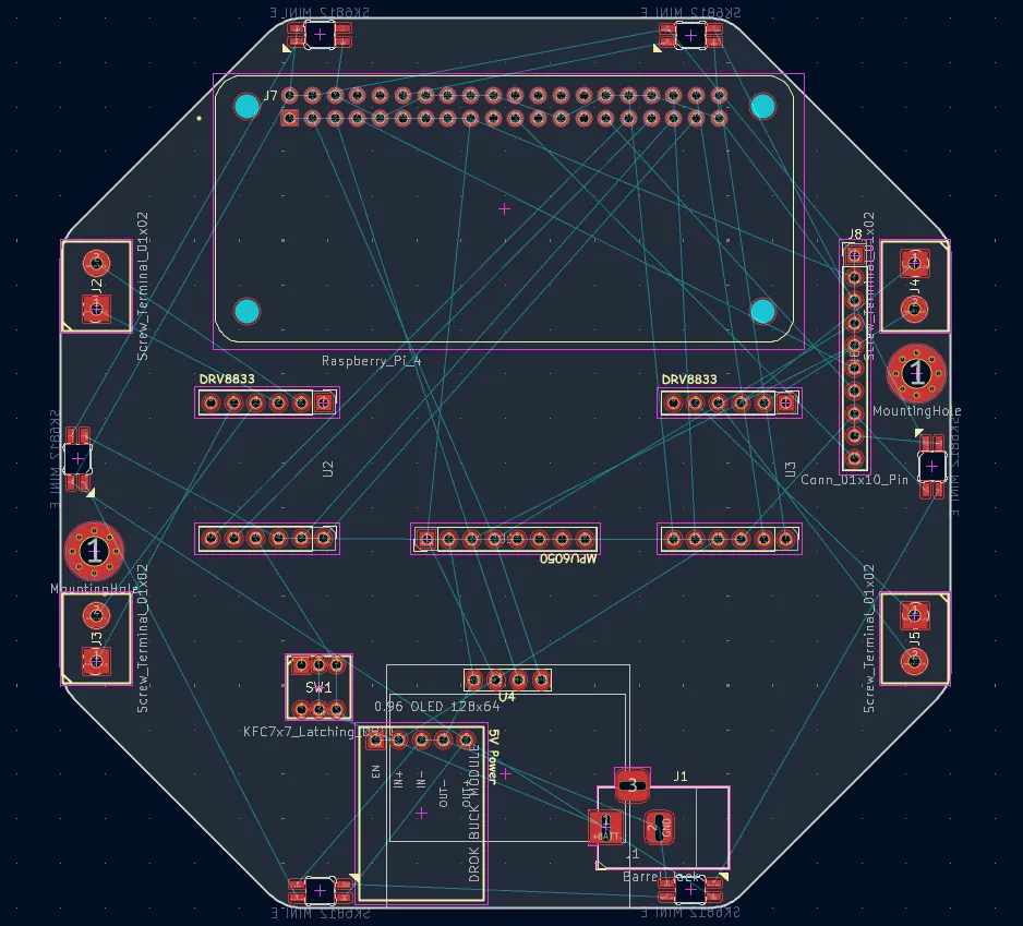
Press F8 to update the PCB from the schematic. KiCad will import the footprints. The thin connection lines are the ratsnest, and the gold/copper pads are the places tracks can start or end.
Press M to move a footprint and R to rotate it. Put connectors near board edges, motor drivers near motor terminals, and the Pi where its USB ports are reachable.
If you want a footprint on the opposite side of the PCB, select it and press F, or right-click and choose Flip. This moves it between the front and back of the board.
Select the Edge.Cuts layer and draw the board outline around your parts. Use the measure tool to check the board size.
Check The Fit In 3D
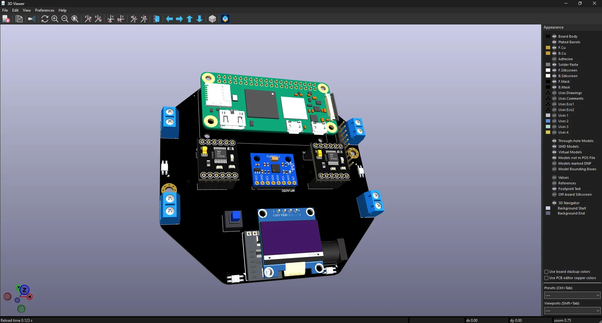
Section titled “Check The Fit In 3D”Before routing, check that the parts physically fit together.
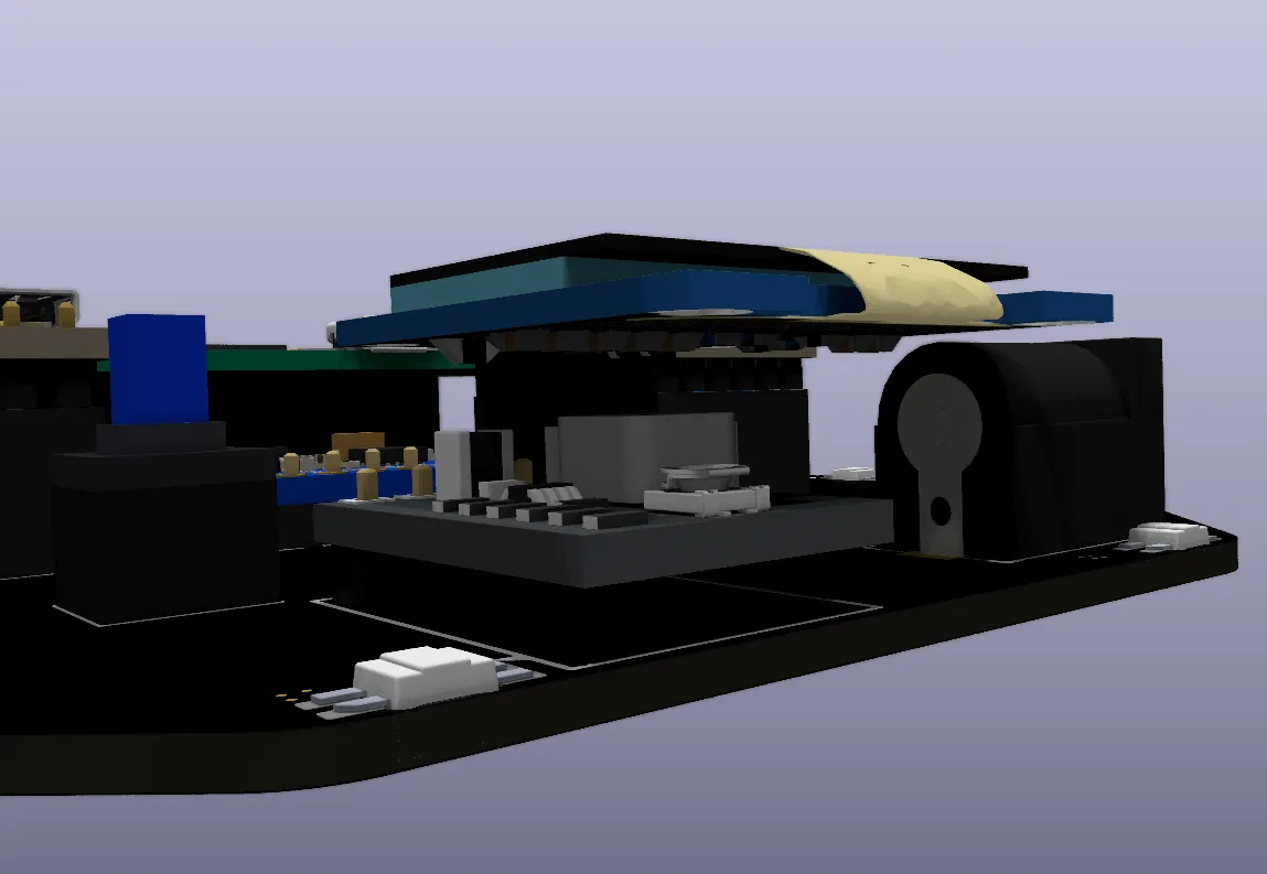
Open View > 3D Viewer. Rotate around the board and look for parts intersecting each other, connectors blocked by other parts, or modules sitting where they cannot actually be installed.
If two parts overlap in 3D, move one of them or choose a different footprint height before you route traces.
Set Trace Widths
Section titled “Set Trace Widths”Set up trace widths before routing so you can quickly switch between small signal traces and larger power or motor traces.
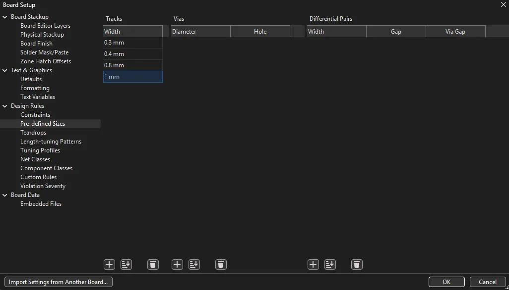
Open the predefined track-width editor from the PCB editor toolbar.
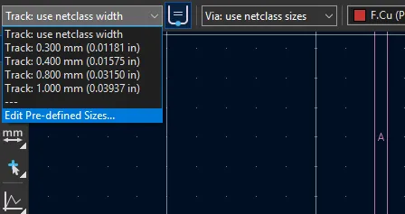
Add at least one normal width for GPIO and I2C, plus a larger width for motor and power connections. During routing, pick the width that matches the connection you are drawing.
Add A GND Pour
Section titled “Add A GND Pour”A GND copper pour fills empty board space with copper that connects to GND. It can simplify routing because many ground pads connect to the pour instead of needing individual ground traces.
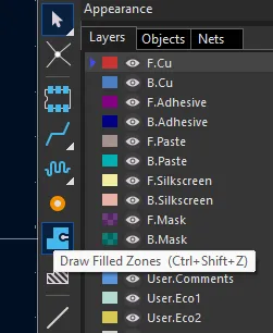
Click the copper-zone tool.
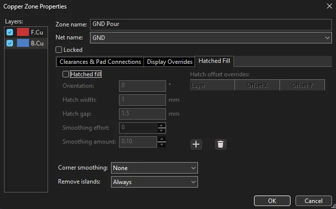
Set the net to GND, choose both copper layers, and draw the zone around the board area. Press B to refill zones after you create or edit traces.
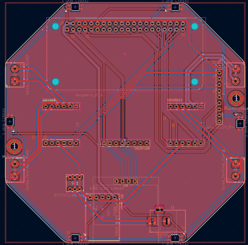
Route The Board
Section titled “Route The Board”Routing turns the ratsnest into copper tracks.
Press X, click a connected pad, follow the ratsnest, and click the destination pad. Use F.Cu for front copper and B.Cu for back copper. If you need to change layers while routing, press V to place a via.
Use the wider predefined trace width for power and motor paths. Use the smaller width for GPIO and I2C.
Polish And Check
Section titled “Polish And Check”Add silkscreen labels for motor outputs, header pins and your name. You can also add art to make the board feel finished.
Heres examples from my board:
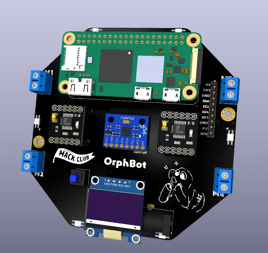
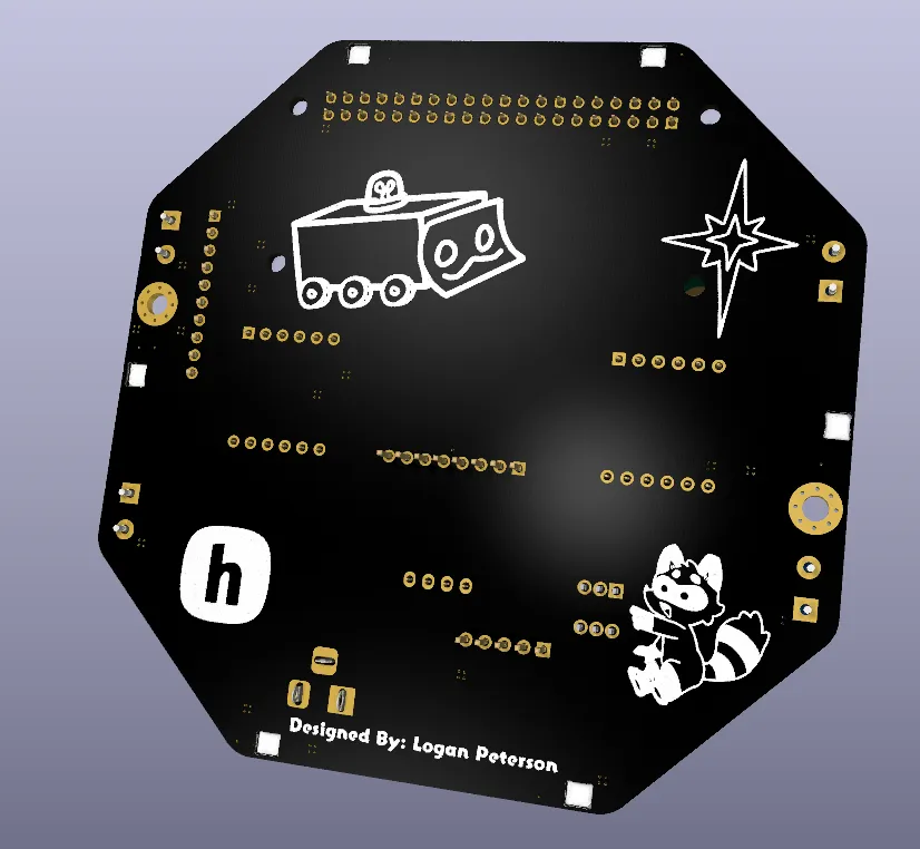
Google KiCad silkscreen art or KiCad image converter silkscreen if you want to get creative; there are tons of tutorials online!
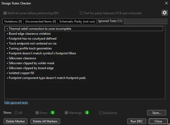
Run Inspect > Design Rules Checker and fix real errors. The example below shows checks intentionally ignored for this board and what a clean no-violations result looks like. Do not ignore unrouted net errors!
That’s it! You now have a routed and ready robot control PCB!